Even solar cells have to slim down. They have to be thinner! But why? And how thin solar cells is it possible to make? This has been the research question addressed by the DiaMApp project, and the following is a presentation of our results.
Thin solar cells mean lower levels of CO2emissions
One of the things we’re looking to reduce is the volume of materials used in the manufacture of solar cells. Most solar cells are made of silicon, which is of one of the planet’s most abundant elements. So, why is it so important to reduce the use of silicon?
Most of the silicon in the Earth’s crust is found in the mineral quartz. Quartz is made up of single silicon atoms bonded to two oxygen atoms, but solar cells can only be made using the pure form of silicon. So the first thing we have to do is to break all the silicon-oxygen bonds and then get rid of twice the number of oxygen atoms as there are silicon atoms in the quartz. We do this by loading the quartz into large arc furnaces together with wood chippings, coal or another material containing carbon. Then we turn on the electricity and out comes silicon and CO2.
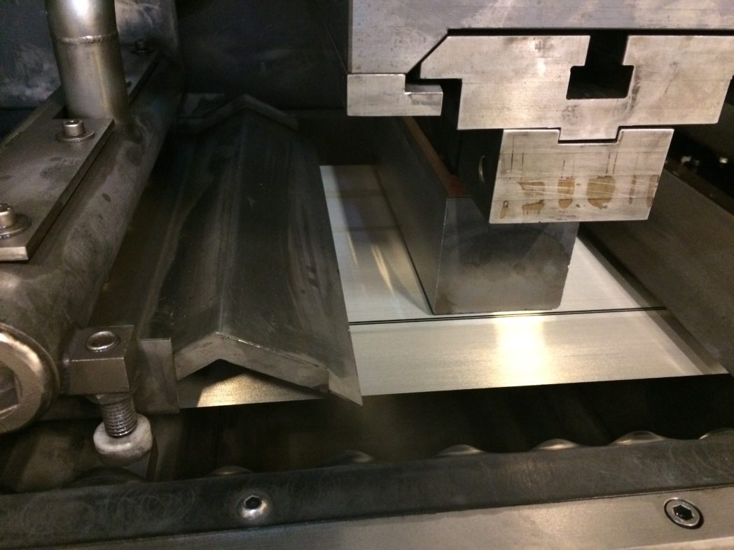
I’ve already mentioned some of the things that most of us agree we should produce and use less of. Firstly, we want to reduce our consumption of coal, and secondly, minimise CO2 emissions. Moreover, a lot of energy in the form of electricity is needed to break the bonds between the silicon and oxygen atoms, and we also want to reduce energy consumption.
- If you want to find out more about how SINTEF is working to make solar cells more efficient, then read this blog (Norwegian):
Pure silicon simply isn’t pure enough
After we’ve extracted the pure silicon from the arc furnaces, we find that it isn’t really pure at all. It is in fact contaminated. That’s to say, it depends on what scale we are talking about and that depends on what we want to use the silicon for. For some applications it wouldn’t be considered contaminated at all.
If we want to add silicon to a steel alloy we may find that it’s more than pure enough, but if we want to use it to make a solar cell it will be much too contaminated. The presence of foreign atoms (contamination) will make the solar cells less efficient. This is why we have to get rid of as many foreign atoms as possible in order ideally to achieve what we call the “nine Ns” – a purity of 99.9999999%. This represents a level of contamination corresponding to the amount of caffeine in a cup of decaffeinated coffee after it is mixed with 10 tonnes of water. There are many ways of purifying silicon, but all of them are very energy-intensive.
Ideally we want to achieve what we call the “nine Ns” – a purity of 99.9999999%.
Fighting on many fronts
Fortunately, we are fighting on many fronts simultaneously. We’re looking into minimising coal consumption, CO2emissions, and energy consumption in the silicon manufacturing process. Work is also being carried out to find alternative ways of purifying silicon. For example, the company REC Solar in Kristiansand can boast the world’s smallest carbon footprint linked to its purification process. But, regardless of how efficient or eco-friendly alternative silicon purification processes are or will become, they will still demand resources and generate by-products.
Another good reason for reducing the consumption of silicon in solar cell manufacture is of course the cost. In order that the green transition can become a reality, the sustainable alternatives must become competitive in the open market.
Eco-friendly alternatives simply have to get cheaper.
How do you manufacture thin silicon?
The key component of a solar cell is a thin wafer of silicon. In modern solar cells, the wafers are commonly about 150 μm thick, approximately the same as that of a strand of hair, and measure 15 by 15 cm square. Silicon is both hard and brittle, making it difficult to cut and easy to shatter. So how is it possible to make wafers measuring 15 by 15 cm, and only 150 μm thick? The secret is to saw them. Yes, you read correctly, we saw them!
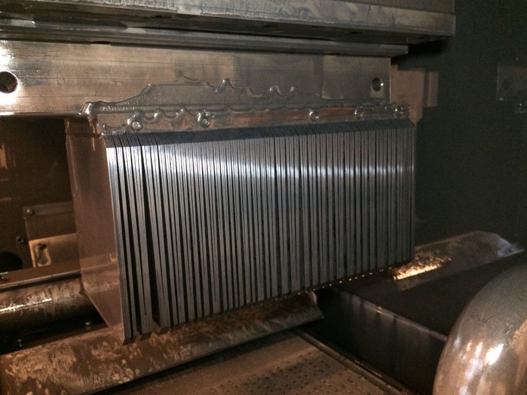
After the long process of extracting the silicon from the quartz, followed by purification, the pure silicon now has to be re-cast. A solar cell requires not only that the silicon is pure, it also has to have all of its atoms arranged in orderly rows – a regular crystalline structure. The silicon crystals manufactured today weigh more than 100 kg and are cut into blocks which are then sawn to produce the thin wafers.
- If you want to find out more about why silicon has to have an orderly crystalline structure, we recommend that you read this blog (Norwegian):
A saw that is able to cut into such a hard and brittle material is no ordinary saw. We use a so-called multi-wire saw. Thin steel wires embedded with minute diamonds are wrapped across two rollers, creating a kind of loom that looks a bit like an egg slicer. Each wire is the same thickness as a strand of hair, and the gap between the wires corresponds to the desired thickness of the silicon wafers, again the thickness of a strand of hair.
As the rollers start to turn, the saw is supplied with copious amounts of cutting fluid. The silicon block is pressed down towards the wires, which then start to scrape away at the silicon. At the other side emerges a large pile of ultra-thin silicon wafers that can then be used to manufacture solar cells. A large amount of silicon dust is also created as part of this process, and makes a grey slurry when mixed with the cutting fluid. Half of the silicon block is discarded in this dirty slurry, like wet silicon sawdust! We are of course working to find a way of recycling this slurry, but at present most of it goes to make concrete filling additives. Perhaps there’s no need to say that no-one wants to see such a valuable material ending up as a filling additive.
So, it isn’t just the thickness of the silicon wafers we’re trying to reduce, but also the gap between them. The steel wire loom is so dense and delicate that it most resembles a nylon stocking.
How thin is it possible to saw silicon?
So, thin is good, and in terms of reducing materials and energy consumption, the thinner the better. But how thin is it possible to make the wafers? Of course, we can’t make solar cells from infinitely thin wafers, although this is one of the things we are investigating using another approach. If it was possible to use infinitely thin wafers in a solar cell, how thin can we saw the original block using a loom made of ultra-thin steel wires? Is there a limit, or is it just a question of optimising the process?
At our lab (the Solar Cell Silicon Wafering Laboratory) we have installed an (almost) industrial-scale multi-wire saw. We’ve conducted many experiments, most of which have been unsuccessful. At least, they appeared to be unsuccessful. We had no problem in sawing wafers to 140 μm thick (current industrial solar cells use wafers that are about 150 μm thick), but were unable reduce the thickness to 100 μm. Why?
What difference does 40 μm make?
In order to answer this question, we have to take a closer look at what went wrong when we tried to produce wafers 100 μm thick. The first thing to say is that it wasn’t just that we didn’t succeed – every experiment was a catastrophe! Catastrophe struck just millimetres after the steel wires had begun to eat their way into the silicon block. The wires broke, the block was damaged and the experiment had to be shut down. Since it takes more than 24 hours to clear up after such a catastrophic experiment, and a further 24 hours to get another one started, you can imagine that we experienced some frustrating days in that lab. We did this seven times!

We adjusted the parameters for every new experiment. We sawed carefully, we sawed hard and we sawed slowly. We tried almost everything. But to no avail. Of course, the main question was why did we find it relatively easy to saw wafers 140 μm thick, but entirely impossible to produce them at 100 μm? Does 40 μm really make that much difference?
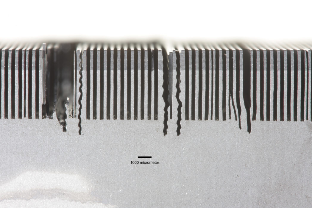
We examined the damaged blocks and discovered that each small cut that the steel wires started to make was the result of the action of either two, or sometimes three, wires. The wires had simply combined, into pairs at least. In some cases we observed triple wire cuts. These sawed in a zig-zag pattern that almost immediately cut into the saw path of the neighbouring wire. This caused small silicon fragments to crumble away, which in turn damaged the thin steel wires. After this, there was no way of avoiding catastrophe. Every time!
Capillary forces – the root of all our problems
Of course, we were then left with the question of why the wires came together instead of remaining in their correct positions as single wires in a well-ordered loom? We discovered that the answer lay in the phenomenon of capillary forces. In order to cool the saw, we had to use a cutting fluid. This fluid, which is commonly water-based, cools the area around the saw and rinses away the silicon saw dust.
The fluid has a surface tension, and in water-based fluids this is quite high. Surface tension is the property that enables pond skaters to walk on water, and capillary forces are those that enable large trees to transport water to the leaves high up in their canopies. If you place a drinking straw in a glass of water, you’ll see that the water creeps up the inside of the straw, making the water level inside the straw higher than that in the rest of the glass. Capillary forces also act on porous materials enabling you, for example, to mop up spilled liquids using a paper towel. We encounter this phenomenon every day, but perhaps don’t give it too much thought.
When we started to compute the capillary forces acting between the thin steel wires of our multi-wire loom, we discovered that they were strong enough to hold two wires together, and that they suddenly became strong enough to achieve this within the range of our attempts to saw 140 and 100 μm thick wafers. Other saws would have reached their own “magic” limits in terms of the thickness of wafer they might produce. The limit will depend on factors such as the distance between the rollers around which the steel wires are wrapped, and the surface tension of the cutting fluid. However, the most important parameter is the distance between the wires or, in other words, the thickness of the wafers we want to produce.
Applying our lessons learned to the future manufacture of thin solar cells
Nature has placed limits on the thickness of wafers we can manufacture using our saw. We can make some adjustments, but all experiments will encounter a “magic” limit, which in fact isn’t magic at all once we understand why the limit is where it is. This little piece of the research puzzle can be used in future to design new multi-wire saws for the manufacture of even thinner silicon wafers.



Comments
No comments yet. Be the first to comment!